Welcome to my personal webpage. | home
Driver Amplifier and Low Pass Filter | Butterworth Low-Pass Filters and Applications of Spectrum Analyzer | BJT Amplifiers | MOSFET CS Amplifiers with Active Load | Common Emitter Circuit | ACCELEOMETER SENSOR | Diode Waveform Shaping | Electronics Projects
Common Emitter Circuit
EE 310 Electronics Circuit Design
Fall 2001
Experiment 6
October 24, 2001
Nima Moshtagh
Introduction
We will be studying the behavior of transistors in the common emitter mode that is the case when the emitter of the transistor is grounded. In this lab we are going to investigate both large-signal and small-signal features of a bipolar junction transistor (BJT). The BJT used in this experiment is a 2N3904 silicon npn transistor. This transistor is a general-purpose device having a fairly large breakdown voltage (BVCBO and BVCEO) and is intended for amplifier applications. The device is not intended for fast logic because it has relatively large capacitance and stores considerable charge when saturated.
In task A we observe the large signal input-output characteristics and the transient response of a CE stage. The second part of the lab designed to study the active region of the transistor including small-signal voltage gain and to improve this voltage gain using different values of resistors.
Part A
Large Signal Characteristics of a CE Stage
We use the circuit of figure 1-a to show the output-input characteristics of the transistor. The Thevenin equivalent of the left part of the circuit is calculated and the simpler circuitry is shown in figure 1-b. Input Vac is 20 Vp-p triangular wave at about 50 Hz.
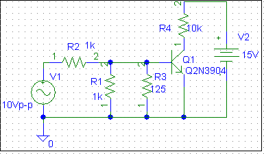

Figure 1-a) Common emitter test circuit 1-b) Thevenin equivalent
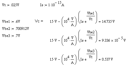
Input (Vbe) is on the X-channel and the output (Vce) on Y-channel. The resulting display (Attachment A) is a representation of the transfer characteristics of the CE stage. The transfer graph or Vce vs. Vbe can provide us with information about three different regions that a transistor can work. At the region that Vce or output is 15 V, the collector current (Ic) would be zero; hence emitter and base currents should be zero and transistor is in cut-off region. The second region with a sharp slope is called active region. In active region of a common emitter stage Vbe should be almost 0.7 V. The output, Vce, can vary in the range of 0-15 volts, before the transistor falls in the cut-off region. If Vbe gets larger than 0.7 V, since Ic is exponentially proportional to Vbe by, the large value of the current through the Rc causes that Vce drops below Vbe and almost equals zero. This case is called saturation. The supportive calculations show the values of Vce (output) for different values of Vbe.
The gain in the active region would be:
Gain = dVce / dVbe » 15 / .125 = 120 (V/V)
To estimate the gain when Vce is near its maximum value, I used the graph in the attachment B that is the same graph as attachment A but larger to get better approximation.
Lowest Gain = (1V) / (0.05 V) = 20 V/V
The highest voltage gain corresponds to the steepest slope of the Vce vs. Vbe plot:
Highest Gain = (2V) / (.0125V) = 160 (V/V)
Transient Response
In the second part of the task A we only need to make some small changes in the input source. A square wave at the frequency of 50KHz is applied to the circuit. To find the exact value of Vac that puts transistor in the saturation region, we change the amplitude of Vac. The maximum value of Vac to get Vce without any clipping is 6.94
volts (Look at attachment C ). When Vbe switches from -6.94 to +6.94 the transistor goes from cut-off (15 volts) to saturation region (0 volt).
An important thing that needs more attention is that the rise and fall times are quite different in the plot of Vce. Slow rise time and fast fall time is typical of the CE state large-signal transient response. The collector output always has parasitic capacitance to drive; some of this comes from the BJT itself and some of it comes from the wiring and any circuits tied to the load, including the oscilloscope probe. The fall time is quite fast because there is an abundance of collector current to discharge the load capacitance into the BJT and pull VCE downward toward ground. However, the rise time is slower. When the BJT is cut off, the only source of current available to pull the collector up is from the resistor Rc. Since the resistor is usually quite large, it cannot rapidly charge the collector load parasitic capacitance, so VCE rises up rather slowly.
From the observed waveform and the known value of Rc, we calculated the capacitance that is apparent at the collector of the transistor.
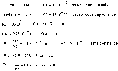
The capacitance of the transistor is found to be 74.3 pF.
Part B
Small-Signal Voltage Gain
The first choice that must be made is to decide exactly where to operate along the VBE-VCE curve. Two factors are important:
1. Bipolar transistor current gain b is somewhat collector current dependent. We want to operate the transistor near its optimum (maximum) value. The data sheet shows that b is at its maximum value (100) when Ic » 10mA (at +25 °C).
2. The collector voltage excursions can be rather large. We want to avoid clipping at both extremes of the output voltage swing. Therefore it is logical to try to center the dc collector voltage operating point VCE near the middle of its range, that is, near Vcc/2 = 7.5 V. This is probably not the region where the large signal trace is steepest.
Therefore, we select Rc so that the optimum DC collector current will flow when the DC collector voltage is Vcc/2.
Ic = 10mA and Vc = Vcc/2 = 7.5 V
Rc = (Vcc - Vc) / Ic = (7.5 V) / (10mA) = 750 W
To adjust Vc to 7.5 volts DC, we set the ac signal to zero and adjust the base bias voltage Vdc until the DC collector voltage is close to Vcc/2. Measurements showed that Vce is approximately 7.5 V when Vdc is equal to 6.47 volts. The circuit is illustrated in figure 2.
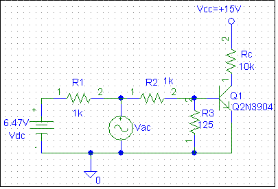
Figure 2) Common-emitter test circuit
To avoid clipping at both extremes of the output swing, we reduce the amplitude of the input so that output signal has a 1-volt peak-to-peak value. Now we can find the Small-Signal AC voltage gain, which is Vce/Vbe. Attachment D displays the input and output at the same time.
Small-signal Gain = Vce/Vbe = 937.5mV / 41.25 mV = 22.7 (V/V)
Improving the Voltage Gain
The goal is to observe the effect of Rc on the voltage gain. By replacing Rc with double Rc (1.5KW) the voltage gain can be measured as:
Gain = Vce / Vbe = 1.031 V / 4.53 mV = 227.5 (mV/V) (Attachment E)
And for Rc = 375 W, the voltage gain happens to be:
Gain = Vce / Vbe = 1.719 V / 4.844 mV = 354 (V/V) (Attachment F)
For the explanation of the results the reader can refer to the Explanation section.
Explanation of Results
In the first part of the task A we found three values for the voltage gain while w used the same circuit in all three parts. The voltage gain near the cut-off region was about 20 V/V; near the saturation region it was about 160 V/V and the overall gain for the active region was measured 120 V/V. Obviously transistor is not a linear device, therefore a designer should be careful to operate the transistor in the segment of active region that transistor behaves almost linearly (Not close to the both extremes of the active region).
In the second part the parasitic capacitance of the collector is calculated to be almost 74 pF, which is large in compare to the capacitance of the breadboard (15 pF) and the oscilloscope (13 pF). This large value of output capacitance makes the rise-time to be slower than fall-time. The reason is that the output resistance Rc is also large; hence the time constant of the discharging circuit is quit large. It means more time is needed to discharge the collector capacitance than charging it.
In part B we tried to increase the voltage gain by changing the output resistance Rc. Since Gain = -gm.Rc one can logically say that by increasing Rc, voltage gain would increase.