Welcome to my personal webpage. | home
Driver Amplifier and Low Pass Filter | Butterworth Low-Pass Filters and Applications of Spectrum Analyzer | BJT Amplifiers | MOSFET CS Amplifiers with Active Load | Common Emitter Circuit | ACCELEOMETER SENSOR | Diode Waveform Shaping Electronics Projects
MOSFET CS Amplifiers with Active Load
Fall 2001
December 6, 2001
Nima Moshtagh
Introduction
In this lab we study one of the basic configurations employed in the design of integrated-circuit MOSFET amplifiers: Common-Source Amplifiers with active loads. Here we employ current sources in place of load resistors. The resulting amplifiers are said to be active loaded, in direct contrast to the usual case of passive loads implemented with resistors. This active load is designed to present a large-valued, AC small-signal resistance to the amplifier while operating under bias conditions, consistent with a much smaller DC resistance. Hence, the circuit can operate with reasonable power supply voltage values and with relatively small power dissipation, while the AC gain theoretically can be quite large.
Two different circuits will be used as active loads to implement an enhancement-type NMOS CS amplifier. In the first part a PMOS current mirror forms the active load and in the next part an additional enhancement-type NMOS FET will be employed.
A) NMOS and PMOS parameters
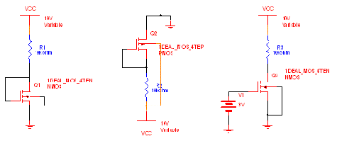
We need to measure threshold voltage (Vt), Early voltage (Va) and the constant mCox(W/L) for both NMOS and PMOS devices. In order to measure Vt for NMOS, we use circuit of Fig 1.a. Note that this circuit is always operating in the saturation region, because the required condition holds for all the times. Since Vds = Vgs the saturation condition (Vds > Vgs - Vt) results in Vt > 0, which is correct for enhancement-type NMOS.
Procedure
First we set Vdd to zero volts (NMOS is OFF). As we increased Vdd nothing happens till a small voltage of 10mV appeared across R. At this point Vgs was near 1.5 volts. The following equation that governs the behavior of a MOSFET in the saturation region shows that when Vgs = Vt, drain current is zero.
To find Early voltage (Va) we set up the simple circuit of Fig.1.c with a fixed gate voltage (Vgs = 3 V). By varying Vdd and measuring current Id, we can get the graph of Id vs. Vds. And we know that: V (drain) = Vdd - V (resistor). Graph 1 show the I-V relationship of the NMOS and Graph 2 is used to find Va using the equation of the straight line in the saturation region.
(a) (b) (c)
Fig.1.a) NMOS with feedback 1.b) PMOS with feedback 1.c) NMOS without feedback
VDD
|
Vds
|
ID (mA)
|
k'
|
Region
|
15
|
9.3
|
0.57
|
0.439971
|
Saturation
|
13
|
7.4
|
0.56
|
0.444199
|
|
11
|
5.6
|
0.54
|
0.43985
|
|
9
|
3.7
|
0.53
|
0.444315
|
|
7
|
1.9
|
0.51
|
0.439715
|
|
5
|
0.6
|
0.44
|
-
|
Triode
|
4
|
0.4
|
0.36
|
-
|
|
3
|
0.3
|
0.27
|
-
|
|
2
|
0.2
|
0.18
|
-
|
|
1
|
0
|
0.1
|
-
|
|
Table 1- Some data points gathered from NMOS in Fig.1.c
To find k' = mCox*(W/L) we just need to plug some data points in the following equation: 
We can repeat the same experiment with a PMOS and here is the summary of the NMOS and PMOS electrical properties:
NMOS
|
PMOS
|
|
Threshold Voltage (Vt)
|
1.5
|
-1.4
|
Early Voltage (Va)
|
-61.3
|
-61
|
mCoxW/L (mA/V2)
|
441.6
|
426.9
|
Table 2- Summary of the NMOS and PMOS parameters.
As we can see NMOS and PMOS are matched in CD4007 and they have almost the same electronics parameters.
B) CMOS Amplifier with Current Mirror
The circuit shown in Fig.2 (known as current mirror) is used in the first part to bias the amplifier circuit. Since Vgs1 = Vgs2 and also both PMOS are the same, then if we want Q2 to operate in the saturation region, drain current (Id) should be equal to Iref. To obtain a suitable value for Iref we just need to adjust current Iref by using a variable resistor (pot).
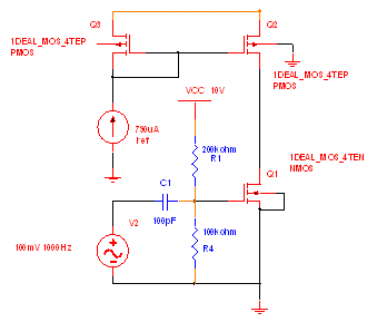
Fig. 2. CMOS Current Mirror
Graph 3 shows the input-output relationship for a current mirror and theoretically both Q1 and Q2 must operate in region III to be saturated. We will experimentally show that this is really the case. Now that we are sure that Q1 and Q2 are saturated we should adjust Vg3 to keep Q3 in the saturation region. Also the DC potential at the amplifier's output node should be set so that it can have a good AC output voltage swing. Since a power supply of 10 V is used as Vdd, we try to keep the DC voltage of the output close to Vdd/2 = 5 volts. The bias circuit attached to the Gate voltage of Q3 produces 3.3 volts at the gate (Vgs) and 4.3 V at the output (Vds). The current (Id) can be calculated as follows:
Vt = 1.5 V Vgs = 3.3 V Vds = 4.3 k'(W/L) = 220 ma/V2
Id = k'(W/L)*(Vgs - Vt)^2(1+Vds/Va) = 720mA
The experimental value was 790 mA that is very close!
C) CMOS as an amplifier
When one applies a small-signal sinusoidal voltage to the input of our circuit and measure the associated output voltage, one can see that it works as an amplifier. Graph 4 shows that the gain of the circuit is equal to -18.4 [V/V].
Small-signal voltage gain = Vout / Vin = 5.188 / 0.2812 = -18.4 [V/V]
One can also find the voltage gain theoretically:
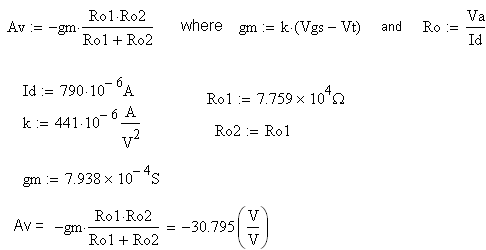
The value of voltage gain that we obtained here is based on the measurements we have done in the previous part and there are definitely some errors, but it's still close to the measured value. This voltage gain is found to be bias dependent:
Iref = 210mA => Av = -21.6 [V/V]
Iref = 790mA => Av = -18.4 [V/V]
Decreasing the drain current (Iref) has increased the gain. Therefore gain (Av) and Id are inversely dependent.
The transfer characteristics of the amplifier is shown in Graph 5 and the large signal gain (d Vout / d Vin) is calculated -19.9 [V/V]. The slope is evaluated in the region of the largest magnitude. This region is where the amplifier previously was biased and operated as a small-signal amplifier.
Large-signal gain = Vout / Vin = -1.922 / 0.0965 = -19.9 [V/V]
NMOS Amplifier with Enhancement Load
Figure 3 shows an NMOS amplifier with an enhancement load. The voltage transfer characteristic, Vout versus Vin, can be obtained as it is sketched in Graph 6. Although the load transistor Q2 operates in saturation at all times, the amplifying transistor Q1 can be operated in cutoff (segment I), in saturation (segment II), or in the triode region (segment III).
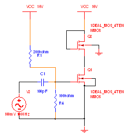
Fig 3. NMOS Amplifier with active load
We used the same circuit to bias the amplifier and to have a DC offset voltage of 4.3 V at the output. For a small signal of Graph 7 the small-signal gain is measured:
Small-signal gain = Av = (Vout)p-p / (Vin)p-p = -196.9 mA / 306.2 mA = - 0.643 [V/V]
The negative sign indicates that the output is 180 degrees out of phase in respect to the input and the magnitude of the gain is less than unity.
To explain the reason of this small gain, first we should consider that since the source gate of the transistor Q1 is not connected to ground, body effect is present in this case. Small-signal gain is calculated to be:
Av = - gm*(Ro1 || Ro2 || (1/gm) || (1/gmb)) » - gm*((1/gm) || (1/gmb)), therefore
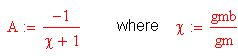
Usually, Ro1 and Ro2 are so large that we can neglect them in parallel to 1/gm and 1/gmb.
Av = -0.64 => X » 0.55 therefore gmb » 0.55*gm.
The small-signal gain of an NMOS amplifier is independent of bias values. We replace 100kW resistor in Fig.3 by a 110 kW, thus Vgs became 4.17 V but the gain didn't change (Look at Graph 8).
The large signal transfer characteristics of the NMOS amplifier is illustrated in Graph 9 and is equal to:
Large-signal voltage gain = Vout / Vin = -0.604 [V/V].
Summary and conclusions
a) Dependency of small-signal gain on Bias conditions
For a CMOS amplifier the small-signal gain is dependent on bias voltage and it can be expressed in terms of gm and Ro as:
Av = -gm*(Ron|| Rop) where
If we decrease Id, Ro increases and on the other hand gm decreases. Since (Ro á 1/Id) and (gm á vId) the effect of Ro dominates. Therefore to improve the small-signal gain we should try to make Id as small as possible.
For an NMOS amplifier, the small-signal gain is independent of bias voltages. The reason is that the ratio of X = gmb/gm is a constant; hence voltage gain must be a constant also.
b) The Width Ratio
We measured k'(W/L) for both NMOS and PMOS and found almost equal values for them. Therefore
Assuming NMOS and PMOS have comparable channel lengths, we can find the width ratio:
We know that (mp » 0.4 mn) thus Wp » 2.5 Wn.
c) Body Effect
In small-signal analysis of CMOS amplifier, source gates of transistors are all grounded, so there is no body effect involved. But for an NMOS amplifier source of the active load is not grounded and there is a voltage difference between base and source; thus an extra term 1/gmb is added in the gain equation that reduces the gain magnitude by more than 30% in our case.