Welcome to my personal webpage. | home
Driver Amplifier and Low Pass Filter | Butterworth Low-Pass Filters and Applications of Spectrum Analyzer | BJT Amplifiers | MOSFET CS Amplifiers with Active Load | Common Emitter Circuit | ACCELEOMETER SENSOR | Diode Waveform Shaping
Driver Amplifier and Low Pass Filter
EE 403W
Spring 2003
Nima Moshtagh
Introduction
A simple Speaker can be modeled by a small resistor. Since the resistance of the device is small, it will draw lots of current when a large voltage is applied across it. A microcontroller that gives the command voltage cannot provide enough current to the speaker, thus a driver is required. When a driver is added, the speaker draws current from a different source than from the microcontroller. In this lab experiment, we are going to design a driver amplifier with the unity gain that will drive an 8§Ù resistance speaker.
Design Specifications
Driver
The desired specifications for our driver amplifier are as follows:
Dissipated power (in the speaker): 1 Watt
Input Signal: sine wave with f = 400Hz
Avg. DC voltage: 0 Volt
Gain: Unity, Non-Inverting
Low-Pass Filter
For high-frequency noise removal a low-pass filter was implemented with these specifications:
Filter Order: 2
Cutoff Frequency: 5 kHz
DC Gain: Unity
Design Procedure
Because the speaker was not supposed to draw any current out of the source (e.g. microcontroller), we used an opamp to build a unity-gain amplifier (figure 1). For a test signal of 4 volts peak, the current through the load was only 26 mA. We calculated the power dissipated in the load using this formula:
This power is much smaller than the desired value. For an 8§Ù load, we can calculate the amount of current that must be provided for the load:
In order to dissipate 1 Watt in the load, a current of more than 350mA is needed. Obviously, a simple amplifier cannot provide enough current to have 1 Watt power being dissipated in the speaker. Therefore, we needed to put a buffer driver that provides current for the load while it would not change the gain of the system.
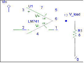
Figure 1. A unity-gain amplifier cannot provide enough current for the load
A high-power, high-current buffer can significantly improve the opamp drive. Figure 2 shows the buffer that we used in conjunction with the amplifier circuit. For our purposes simple transistors like TIP-31 and TIP-32 would do the job, but if the load current is going to be more than 2 amps then TIP31/32 are not good choices.
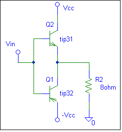
Figure 2. A high-power, high-current buffer using TIP-31/32 transistors
When Vin is positive (first half of the period), TIP-31 that is an npn transistor is ON and TIP-32 (pnp transistor) is OFF. Therefore, a current will flow from the +Vcc through the npn transistor and the load. During the other half of the period, when Vin is negative, TIP-31 is OFF and the current will flow in the other direction, i.e. from the load to the pnp transistor and -Vcc. When Vin is changing sign and its magnitude is very small, neither transistors can be ON. Due to that fact, we expected to see some crossover distortion in the output signal. But we could not detect any distortion.
It can be shown that the maximum power will be dissipated in the load if (see attachment A for detailed calculations). In that case the maximum power dissipated in the load is
 . Because we need to have 1 Watt delivered to the load (P = 1 Watt), Vcc should be at least 5.65 volts (Derivations are provided in appendix A). This voltage was too low and we observed clipping in the output. So, in order to overcome this problem we had to use a higher voltage for Vcc. Vcc = 7.68 volts gave us the current of 350 mA in the load which is what we wanted.
Note: Initially we made the circuit to work with two separate sources: one for running the opamp and another one for buffer transistors. It turned out that it wasn't a good idea to do so and our circuit didn't work. Therefore, we decided to use the same power source for both opamp and buffer transistors.
For noise reduction and avoiding current spikes in the circuit, we put some small capacitors near the voltage sources (see figure 3). Ceramic capacitors below 0.01µF have very good high frequency characteristics, and they are able to act as a local power source for very fast load current spikes.
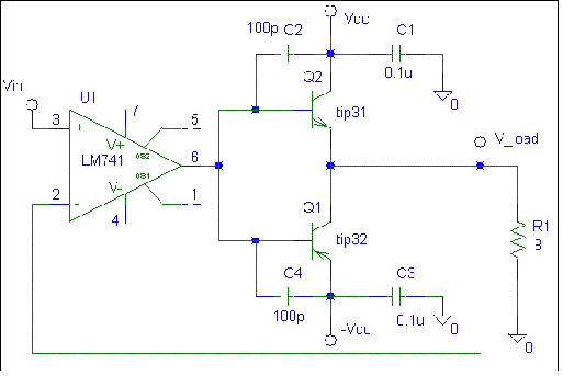
Figure 3. Capacitors are put is parallel to the voltage sources to avoid noise and current spikes.
Low-Pass Filter Design
The signal out of the generator is quite clean, but practical sources may not be so. Therefore, after we got the amplifier working well, we incorporated a 2-pole low-pass filter that has a cutoff frequency of 5kHz. The purpose of this filter is to remove the unwanted higher frequencies that might be present in the input signal.
The filter is a Butterworth low-pass filter which has the flattest frequency response in the passband. Figure 4 shows the filter that we used in our driver amplifier. The DC gain of the filter was more than unity, thus we had to use an attenuator to bring the gain down. The attenuator is just a simple voltage divider. See attachment B for filter design calculations.
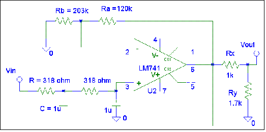
Figure 4 A Low-Pass Filter with Voltage Attenuator
Because our amplifier works at low frequencies (f = 400 Hz) and the low-frequency gain of the entire system (LP filter, amplifier and the driver) is unity, there was no attenuation in the input signal. In other words, input and output signals were exactly the same (See figure 5 and 6 for the comparison of input and output signals). We didn't observe any crossover distortion in the output signal.
Design Verifications
The very first thing of which we needed to make sure was to see if the power dissipated in the load (speaker) is 1 watt or not. We made the following measurements:
which is very close to our desired value.
We varied the power supply voltage to find the best value for our design. The minimum voltage at which no clipping occurred was Vcc = 6.26 V. For voltages smaller than 6.26, we saw clipping in the output signal. On the other hand, as we increased Vcc, transistors became hotter. At Vcc = 7.68 V, the current through the load was 350mA and P=1 Watt. As we increases the frequency of the input signal, the current went down and consequently the dissipated power in the load became smaller. Table 1 shows some measurements.
Frequency (Hz)
|
Current (mA)
|
Power (Watts)
|
400
|
350
|
1.0
|
1100
|
350
|
1.0
|
1500
|
340
|
0.96
|
3500
|
330
|
0.93
|
Table1. Dissipated power decreases at higher frequencies of the input.
As long as the frequency was less than 1100 Hz, the power delivered to the load was 1.0 Watt. Table 1 shows that the power decreases by increasing the frequency of the input signal.
Another goal of our design was to have a unity gain amplifier. In order to show that input and output signals were actually the same, we plotted DC transfer curve (Vout / Vin) of the entire circuit (see Figure 7). The slope of the line is 1 which means that Vout = Vin. Our circuit satisfied all the design specifications.
Conclusions and Discussions
We designed a driver amplifier and a low-pass filter for running a speaker with a small resistance of 8W. Since just an amplifier won't provide enough current for the load, we designed a high-power, high-current buffer circuit by using transistors to drive the speakers with 1 Watt. We calculated that the required Vcc to be 5.65 V if we want to deliver the maximum power to the load. But with Vcc = 5.6 V clipping occurred in the output signal, thus we had to raise the voltage to 7.68 V. The clipping occurred because Vcc was too small for running the opamp.
Our circuit had a low-frequency gain of 1. We added a low-pass filter with Wc = 5kHz to our design to remove high-frequency noise. We didn't observe any change in the output signal because our input signal had a frequency of 400Hz which falls in the passband region of the LP filter.
As we increased the frequency of the input signal, the current in the load dropped and the dissipated power went down. At high frequencies the impedance of capacitors decreases and therefore they would draw a little current from the source. Consequently, less current will go through the load. Finally we observed the DC transfer curve (Vout/Vin) which explicitly showed that input and output signal are equal.