Welcome to my personal webpage. | home
Driver Amplifier and Low Pass Filter | Butterworth Low-Pass Filters and Applications of Spectrum Analyzer | BJT Amplifiers | MOSFET CS Amplifiers with Active Load | Common Emitter Circuit | ACCELEOMETER SENSOR | Diode Waveform Shaping | Electronics Projects
Diode Waveform Shaping
EE 310 Electronics Circuit Design
Fall 2001
October 17, 2001
Nima Moshtagh
Introduction
Using the characteristic of diodes that only conduct when they are in the forward bias, we are going to measure some different signal properties of a given waveform, specifically, the peak-to-peak voltage, the DC offset and the maximum value. The properties of the input signal are as follows:
(a) The peak-to-peak amplitude, not well defined, varies in the range of 4-6 V
(b) The waveform frequency is in the range 500-1,000 Hz
(c) The waveform has a DC offset value in the range of 0-1 V.
Assuming that this square-wave signal needs to drive additional circuitry having relatively tight input level requirements, we design a wave shaping circuitry to clean up the amplitude characteristics of the waveform. Specifically, it is desirable to produce a square wave of the same frequency and having corresponding low and high levels at 0 V and 5 V, respectively.
Design Description
Peak-to-peak Voltage
Before starting the design, we should consider the output characteristics of the clamping circuit. The output of the clamping circuit of figure 2 is always positive and it has it lowest peak clamped to zero volts. The maximum value of the output is equal to the peak-to-peak voltage of the input waveform. Even the presence of a DC offset in the input would not change the low and high levels of the output.
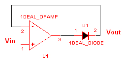
Since the diodes we use in the lab are not ideal, we need to use super diodes to eliminate the loss of voltage across diodes. A super diode is shown in the figure 1.a.
(a) (b)
Figure 1.a) Super Diode b) current voltage characteristics of a super diode
Vin and Vout are equal for a super diode and drawing a current through the diode will provide the required voltage across it. In other words a super diode behaves like an ideal diode. (Figure 1.b)
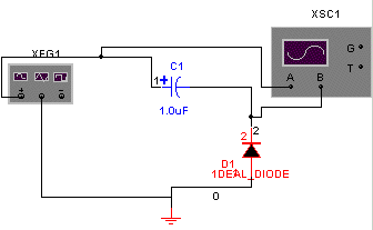
Figure 2) Simple clamping circuit
Having clamped the waveform to 0V, we use a peak rectifier circuitry to keep the peak of the clamping circuit at its high value that is equal to Vp-p of the input waveform. When the input is high, super diode is ON and the capacitor is charging; while it cannot be discharged when the input voltage drops to the lower voltages, because the super diode is now OFF. Therefore the output will be fixed at Vp-p, which is why the circuit called peak rectifier. In both parts of the circuit we used super diodes to avoid the loss of voltage across the diodes.
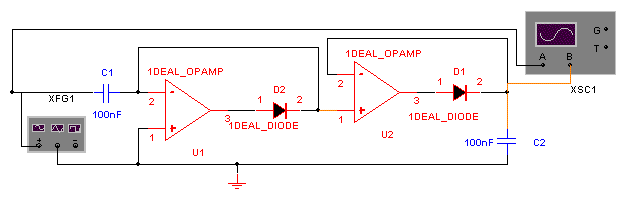
Figure 3) Peak Rectifier Circuitry
Maximum Voltage
The maximum voltage can be simply found by using a peak rectifier circuit (Figure 3) without the clamping circuit. Figure 4 shows the schematic of the circuit we actually built in the lab. The capacitor needs a resistor for discharging. Since the time constant of the RC circuit (t = RC) is 100 sec., the output level will not drop significantly while capacitor is discharging. For large enough values of C and R the output should be equal to the maximum value of the waveform.
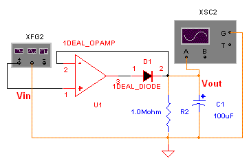
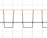
Figure 3) Maximum Voltage Circuitry and the output
Offset Voltage
The circuit of measuring DC offset voltage is very simple. We use this property of the capacitor that it behaves as an open circuit in the presence of a dc signal. When the capacitor is charged, because the time constant of the circuit is too high for the capacitor to discharge, it will keep the output voltage at DC offset voltage. If the time constant t is small, capacitor will be discharging during the low levels of input signal and the output will not be a straight line anymore.
Figure 4) DC Offset Voltage Circuitry And The Output
Wave shaping Circuit
We are asked to produce a clean square-wave signal out of the input waveform having high and low levels at 5V and 0V, respectively. One way to accomplish this could be using a comparator op amp. If we attach a diode to the output of the op amp, we can filter the negative values and generate a totally positive waveform. The output of the diode is swinging between 0V to +15V; therefore a voltage divider is used to make the desired voltage (+5V) at the output.
3
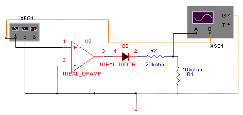
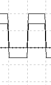
Figure 5) Wave-shaping circuit
When V+ is greater thatn V- (or Vin is positive) the output voltage of the op amp would be positive and diode would be ON and conversely, when Vin has negative values, diode would be OFF and Vout would be equal to 0V.
Results Of The Experiment
For an input signal of 10V peak-to-peak with a DC offset voltage of 1V, the measurements showed that the input signal had the peak-to-peak amplitude of 10.1V and 0.98 dc offset voltage. The maximum value of the input signal was measured 6.1V. The frequency of the input and output signals are 1000Hz.
Conclusions
The very first thing I learned from this lab was that by using a super diode we can acquire the characteristics of an ideal diode. Without using super diodes, all the measurements will be off because of the voltage drop across the diode in the forward bias. The other interesting circuit of this lab was clamping circuit. The output of this clamping circuit is positive at all the times and the reason is that the capacitor is charged when the source has negative values. So the voltage of the capacitor Vc is equal to Vmin. Also capacitor keeps its voltage because it cannot discharge through the diode in the reverse bias. Hence the output would be the voltage of the source plus its minimum voltage (or Vc). Therefore the output cannot be less than zero volts.