Welcome to my personal webpage. | home
Driver Amplifier and Low Pass Filter | Butterworth Low-Pass Filters and Applications of Spectrum Analyzer | BJT Amplifiers | MOSFET CS Amplifiers with Active Load | Common Emitter Circuit | ACCELEOMETER SENSOR | Diode Waveform Shaping | Electronics Projects
BJT Amplifiers
EE 310 Electronics Circuit Design
Fall 2001
November 15, 2001
Nima Moshtagh
Introduction
This experiment investigates the small-signal properties of the three different BJT amplifier configurations common emitter (CE), common base (CB) and common collector (CC). By building all three and measuring their gain and input/output resistances (Rin and Rout) we will be able to compare their relative characteristics and, in turn, be able to learn which one to use when designing an amplifier. Unlike op amps, which are nearly ideal from a circuit-loading standpoint (Zin very large and Zout almost zero), BJT amplifiers have finite input and output resistances and will clearly interact with each other when stages are cascaded together to form multistage amplifiers.
Active Bias
In order to get a transistor to amplify properly it must be biased in its active region. We are going to use active bias instead of passive bias with resistors and capacitors. Active bias with an additional transistor used as a current source is quite common in integrated circuit design where space and fabrication concerns make the use of transistors preferable to passive elements like resistors and capacitors. The other advantage of active bias is that it enables us to construct one bias circuit that can be used on all three types of amplifier configurations (CE, CB, CC) with minimal changes.
In the circuit of Figure 1-a, active bias is used to generate the bias currents in the entire circuit. Measurements showed that current Ic1 is directly proportional to the value of V- and is independent of V+. The table below shows the measurements done on the circuit. The theoretical values of Ic1 for +/-15V and +/-10V are also calculated in attachment 15 and 16 and are included in the table.
V+ (v)
|
V- (v)
|
Vce (v)
|
Vrc (v)
|
Ic1 (mA),
Measured
|
Ic1 (mA),
Theoretical
|
15.0
|
-15.0
|
7.7
|
7.67
|
3.84
|
3.78
|
10.0
|
-10.0
|
5.75
|
4.92
|
2.46
|
2.42
|
15.0
|
-10.0
|
10.80
|
4.92
|
2.46
|
10.0
|
-15.0
|
3.14
|
7.65
|
3.83
|
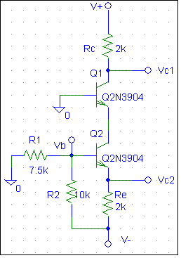
(a) (b)
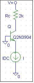
Figure 1 a) Active Bias Circuit b) Active bias circuit works the same as a current source.
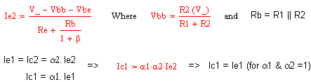
We can show that these results are theoretically correct too. First we should find the Thevenin equivalent of the circuitry attached to the base of the Q2.
Here we note some of the advantages of active bias. First, the collector current of Q1 is approximately equal to IE2; therefore it is controlled and stabilized by the current source (Figure1-b). Stabilizing the current through Q1 is desirable because the hybrid-pi model parameters are bias dependent. Also, it is easy to adjust IC1 if a different bias point is desired just by changing the resistor values.
Common Emitter (CE) Amplifier
The CE stage is the most useful of the three basic configurations and it is the only one that can simultaneously achieve both current and voltage gain magnitudes greater than 1. In this part of the experiment we examine CE stage without unbypassed emitter resistance. At frequency of 10kHz the reactance of the Ce is so small that it may be
considered shot circuit; thus we can say that the emitter of Q1 is directly connected to ground.
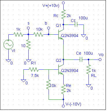
Figure 2) Common Emitter (CE) Amplifier
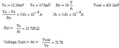
The goal is to measure the input resistance (Ri) and voltage gain (Av) of the transistor. Attachments A, B and C show the measured signals for Vs, Vb, and Vout. Theoretically input resistance is equal to Rp that can be measured experimentally:
Ic = 2.4mA b = 100 Vt = 25mV
Rp = (bVt) / Ic = 1041 W
Another method to measure input resistance is:
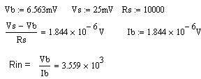
Voltage Gain = Vout / Vin = Vo / Vb = - 315.6mV / 6.563mV = - 48 (V/V)
Q-point for transistor Q1: Ic = 2.4mA Vce = 5.94 V
The above calculations show that CE stage has high voltage gain and rather small input resistance. The negative gain indicates that the output and input signals are 180 degrees out of phase. Increasing the input voltage may cause some nonlinearity. Attachment 4 shows that when Vin is about 5.3 volts, almost 10% nonlinearity can be seen in the output and in addition voltage gain drops to 38 V/V. As the input signal is further increased, waveform clipping ultimately occurs due to the device either going into cutoff or saturation. Attachment 5 illustrates how both forms of clipping occur. At this point voltage is as low as 14.4 V/V.
CE Amplifier with Unbypassed Emitter Resistance
We modify the amplifier in Figure 2 to include a small, unbypassed emitter resistor Re, between the emitter of Q1 and ground. At the first glance, we notice that it takes larger input signal levels for Vi, Vs and Vb (attachments 7 and 8).
Input resistance and voltage gain also take new values:
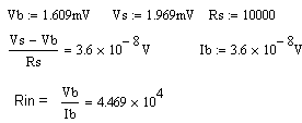 Rin = 44.69 kW
Av = Voltage gain = Vo / Vb = -7.00 / 1.609 = - 4.35 V/V
The same result can be achieved theoretically:
Adding the unbypassed resistor has increased the input resistance Rin by a factor of 12 and decreased Av by a factor of 10. Same as previous experiment, we find the input and output voltages for 10% nonlinearity in the output. Attachment 6 shows both input and input signals overlaid on the scope. The voltage gain jumps to 7.0 V/V.
Attachment 7 shows the point that both forms of clipping occur while we continue to increase input voltage. So at that point Vout (peak-to-peak) won't increase as we increase input voltage.
Common Base (CB) Amplifier
If we detach source from base in the figure 2 and ground the base and apply source to the emitter, we get the common base configuration (Figure 3).
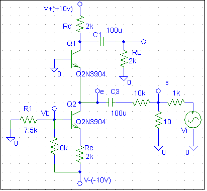
Figure 3) Common Base (CB) Amplifier
Transistor Q2 is still working as an active bias and keeps the operating point of transistor Q1 at the same level:
Q- point for transistor Q1: Ic = 2.48mA Vce = 5.62 V
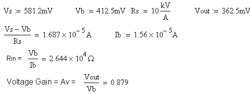
We measured Ve and Vs in figure 3, but there is not much difference between two voltages. This means that the source current is very small. Note that Rs has been reduced from 10 kW to 10 W. In fact, with the input resistance so much smaller, the assumption that Ce can be approximated by a short circuit is probably no longer true.
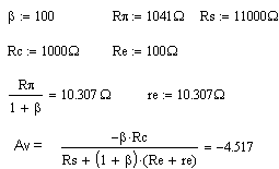
Voltage gain and input resistance of the CB amplifier are equal to:
Low input resistance and high voltage gain are main characteristics of the CB amplifiers. Also common base amplifiers don't have a large current gain:
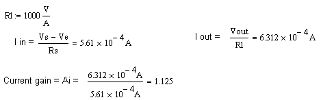
In this calculations R1 = Rl || Rc = 1000 W and Rs = 10 W.
Same as previous experiment, we find the input and output voltages for 10% nonlinearity in the output. Attachment 9 shows both input and input signals overlaid on the scope. The voltage gain would be 54.7 V/V.
Attachment 10 shows the point that both forms of clipping occur while we continue to increase input voltage and it should be as high as 17.7 volts to get both kinds of clipping. In compare to CE stage that clipping occurs at 1.06 volts, CB stage has much higher input level.
Common Collector (CC) Amplifier
The CC amplifier (often called an emitter follower) is configured such that the ac input signal drives the base and the output is taken at the transistor's emitter, as shown in figure 4. We are going to measure small-signal gain and input resistance. A 1-volt peak drives the circuit. Measurements are as follows:
The reason that common collector is called emitter follower, as one can see is that a CE amplifier has a voltage gain of unity and a high input resistance.

Figure 4) Common Collector (CC) Amplifier
The input and output levels at which the onset of clipping occurs are depicted in attachment 11. The clipping at the peak happens when the transistor falls in the saturation region (Vin = +6.3 V). When the source voltage drops to its minimum value, transistor will be cut off and the next clipping will occur at Vin = -6.3 V. The limits at which clippings occur are +/- 5 volts for Vout. This range of output voltage is rather wide, so it's not suitable for driving low impedance loads. In order to decrease the range of changes at the output, we can replace 1k-output resistance by a 100 W resistance.
Attachment 12 shows that both forms of clipping occur while output voltage changes 1.25 V peak-to-peak. Voltage gain is still around unity and input resistance is quit large.
Summary
Here is the summary of what we learned from this lab: